Prodways CERAM PRO Ceramic 3D Printing Solutions by Lodestar 3D
Lodestar 3D is the exclusive distributor of Prodways Printers’ ceramic 3D printing solutions in India, helping manufacturers, foundries, research centers, and advanced ceramic teams evaluate the right CERAM PRO system for production and R&D workflows.
Ceramic 3D Printing Solutions for Indian Manufacturers & R&D Teams
Ceramic 3D printing buyers need more than a product list. They need a workflow recommendation that connects application, CERAM PRO printer selection, ceramic material, software, debinding, sintering, finishing, and production support.
Ceram PRO 365 for high-resolution ceramic workflows with silica and alumina material options.
0nm
Ceram PRO 385 / 385+ for open-material ceramic 3D printing and R&D flexibility.
0 nm
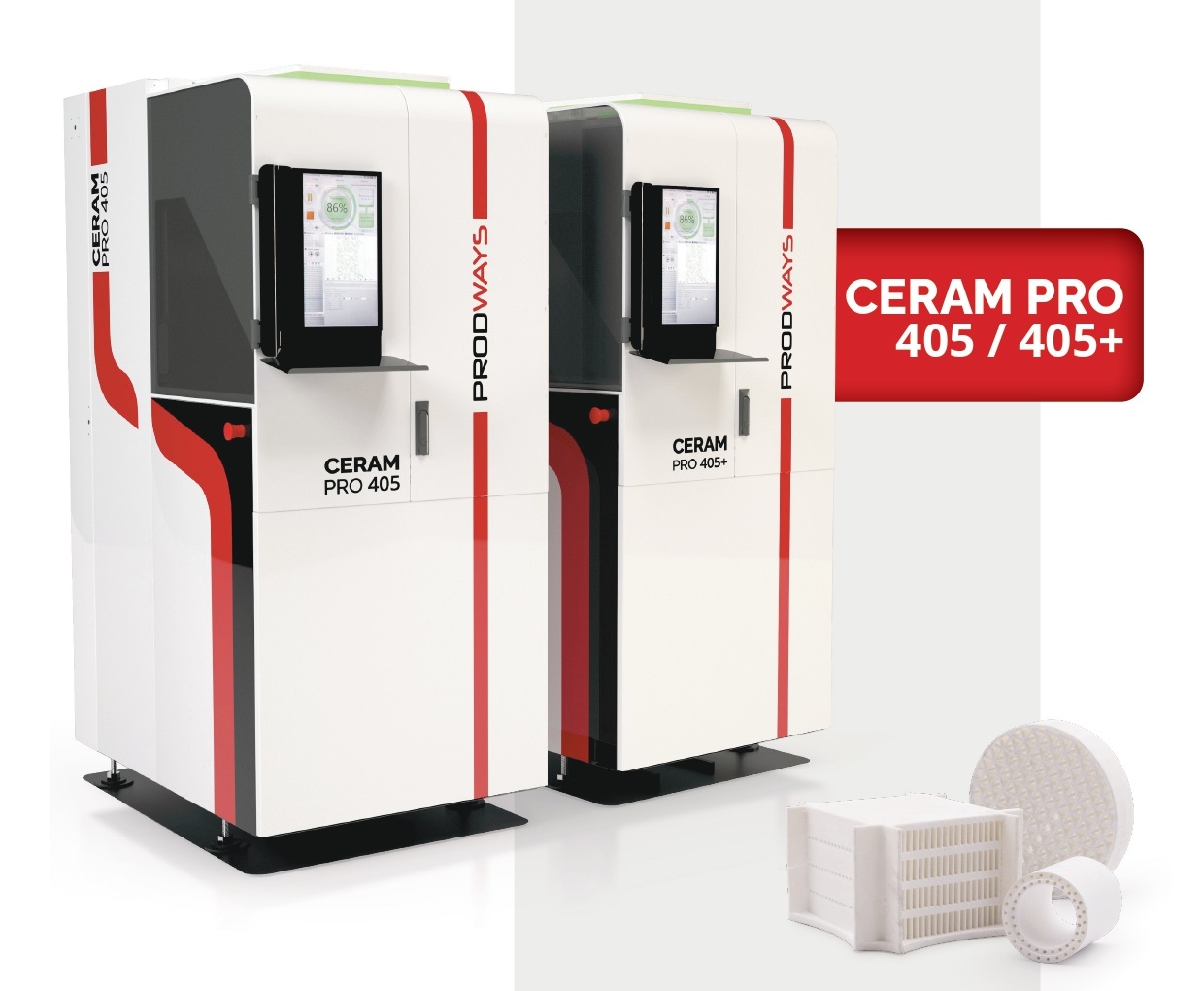
Ceram PRO 405 / 405+ for ceramic applications using 405 nm UV-LED DLP technology.
0 nm
Maximum build envelope available across selected CERAM PRO models, depending on configuration.
300×445×350
Ceramic Additive Manufacturing
What Is a Ceramic 3D Printer?
A ceramic 3D printer creates ceramic green parts from a digital 3D file using a ceramic-loaded resin or slurry. After printing, parts generally move through cleaning, drying, debinding, sintering, and finishing stages to achieve the required ceramic properties.
Prodways CERAM PRO systems use UV-LED DLP technology with MOVINGLight® top-down printing. The range is designed for advanced ceramic applications where precision, surface quality, repeatability, and material control are important.
Complex geometries difficult to manufacture with traditional tooling
Final material properties depend on material selection, print parameters, debinding, sintering, finishing, and quality-control validation.
Why Prodways
Why Choose Prodways CERAM PRO for Ceramic 3D Printing?
Prodways CERAM PRO printers are designed for demanding ceramic 3D printing applications where production flexibility, high resolution, and material openness are important buying factors.
01
MOVINGLight® DLP
Top-down DLP technology supports precise light projection and consistent results across the build area.
02
High Resolution
CERAM PRO 365 offers 31 μm native pixel size, while 385 and 405 models offer 42 μm native pixel size.
03
Open Parameters
Selected CERAM PRO systems are positioned for open-material workflows, making them useful for R&D and material development.
04
Modular Platform
Adjustable build platforms help teams match build volume to part size, batch size, and material usage.
Applications
Ceramic 3D Printing Applications for Indian Industry
Use this section to educate buyers before they compare printer models. Ceramic 3D printing is usually purchased for specific workflows, not only for machine specifications.
Investment Casting
Supports complex ceramic patterns, cores, and casting-related workflows where geometry and detail matter.
Technical Ceramics
Useful for high-performance ceramic parts, prototypes, and functional components after validated firing workflows.
Research & Development
Helps universities, labs, and R&D teams test materials, geometries, and advanced ceramic concepts.
Advanced Materials
Supports experimentation with alumina, silica, and other ceramic material systems where validated.
Aerospace & Defense
Suitable for evaluation in advanced manufacturing workflows that require lightweight, heat-resistant ceramic geometries.
Education & Training
Enables additive manufacturing learning for ceramic materials, DLP printing, debinding, and sintering workflows.
Energy & Industrial
Supports evaluation for insulation, filtration, thermal, and industrial ceramic part development.
Jewelry & Casting
Supports casting-related workflows where high surface quality and detailed features are required.
CERAM PRO Range
Prodways Ceramic 3D Printers Distributed by Lodestar 3D
Each CERAM PRO model serves a different wavelength, throughput, and material workflow requirement. The right choice depends on your application, material, production volume, and validation needs.
Ceram PRO 365
High-resolution ceramic 3D printer with 365 nm UV-LED DLP technology and 31 μm native pixel size. Suitable for silica and alumina workflows and investment casting related applications.
385 nm ceramic 3D printer range for open-material workflows. The 385 model uses a single DLP head, while 385+ adds dual DLP heads for faster throughput.
405 nm ceramic 3D printer range for open-material workflows. The 405+ version uses dual DLP heads for higher throughput compared with the single-head 405 model.
Use this table as a starting point. Final model selection should be confirmed with Lodestar 3D based on application, material, throughput, and installation requirements.
Model
Best Fit
Core Specs
Material / Workflow Notes
CTA
Ceram PRO 365
High-resolution ceramic printing for investment casting, silica/alumina workflows, and technical ceramic R&D.
Single DLP head, 365 nm wavelength, 31 μm native pixel size,
50–175 μm layer thickness, 264 × 328 × 350 mm max build envelope.
Prodways lists compatibility with SILICA SICAST 1200 and ALUMINA A100 resins.
Lodestar lists silica and alumina slurry compatibility.
The buying decision should start with the application, not only the model name. Use this decision guide to route visitors toward the right quote request.
Need silica / alumina workflow
Your project focuses on high-resolution ceramic workflows using listed silica and alumina material options.
Start with: Ceram PRO 365.
Need 385 nm open materials
Your team is developing or validating ceramic materials and wants open-parameter flexibility at 385 nm.
Compare: Ceram PRO 385 / 385+.
Need 405 nm open materials
Your workflow requires 405 nm ceramic printing and application-specific material validation.
Compare: Ceram PRO 405 / 405+.
Need more throughput
Your production plan requires faster output and higher batch productivity.
Consider: 385+ or 405+ dual-head models.
Need application validation
You need help confirming printer, material, debinding, sintering, and finishing fit for your part.